
Positive Voltage Regulator Circuit with PNP Boost

Positive Voltage Regulator Circuit with PNP Boost circuit diagram

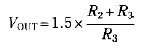
The IC8211 presents the voltage reference and regulator amplifier, although Q1 will probably be the series pass transistor. R1 defines the output current of the IC8211, although C1 and C2 present loop stability and as well act to suppress feedthrough of input transients to the output supply. R2 and R3 define the output voltage as follows:

Positive Voltage Regulator Circuit  circuit diagram

Furthermore, the values of R2 and R3 are preferred to create a bit volume of standing current in Q1, which provides additional stability margin on the circuit.Where accurate setting of the output voltage is needed, either R2 or R3 could possibly be designed adjustable. If R2 is designed become adjustable,then the output voltage will vary linearly with the shaft angle; nevertheless, if the potentiometer wiper was to open the circuit, the output voltage would rise. Normally, for that reason, it is far more beneficial to provide R3 adjustable, due to the fact this can give fail-safe operation.

Comments

Popular posts from this blog

LM317T Voltage Regulator Circuit with Pass Transistor

This is the schematic diagram of voltage regulator circuit with pass transostor. The regulator is based regulator IC of LM317T. The LM317T output current can be raised by utilizing an additional power transistor (on circuit, it is 2N2955) to share a portion of the total current. The amount of current sharing is established with a resistor placed in series with the LM317 input and a resistor placed in series with the emitter of the pass transistor. In the above scheme design , the pass transistor will start conducting when the LM317 current reaches about 1 ampere, due to the voltage drop across the 0.7 ohm resistor. Current limiting happens at about 2 amperes for the LM317 which will drop about 1.4 volts across the 0.7 ohm resistor and make a 700 millivolt drop across the 0.3 ohm emitter resistor. Thus the total current is limited to about 2+ (.7/.3) = 4.3 amperes.

5V to Isolated 5V Converter Circuit

This is the circuit diagram of 5V to Isolated 5V Converter, rated at 20mA electric current. In this converter circuit, a negative output voltage dc to dc converter generates a -5V output at pin A. In order to generate -5V at point A. the primary of the transformer must fly back to a diode drop more negative than -5V. If the transformer has a tightly coupled I : 1 turns ratio. there will be a 5 V plus a diode drop across the secondary. The IN5817 rectifies this secondary voltage to generate an isolated 5V output. The isolated output is not fully regulated since only the -5V at point A is sensed by the MAX635.

Sealed Lead Acid (SLA) 12V Battery Charger with Current Limiting

This is the circuit design of Smart Sealed Lead Acid (SLA) 12V Battery Charger featuretwith Current Limiting. The charger uses a two step process for charging SLA batteries – a current limited ‘fast’ mode followed by a constant voltage ‘float’ mode. Maximum charging current is 1A. An onboard LED indicates when the charger is in ‘fast’ mode. When the LED goes out the battery is charged and the charger has switched to ‘float’ mode.