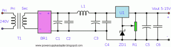
Here a variable power supply circuit which the output voltage can be adjusted. The stabilizer IC may be changed with different value as needed, example 7815 for 15v maximum voltage.
Component Parts List:
T1 Transformer 10:1 Secondary 24V @ 2A
BR1 Bridge Rectifier 50V PIV 2A rating
C1 4700u (35V)
C2 0.001u
C3 2200u (35V)
C4 0.001u
C5 4.7u (25)
C6 0.01u
R1 10k potentiometer
L1 see text
U1 7805 N.B. This may be changed for different output voltages e.g. 7812 for higher output voltage
ZD1 15V zener @ 1.3W
The specific inductance of the ferrite (core)is important. A core should be chosen to work within the specific frequency as stated by the manufacturer. L1 is a powder core and has 32 turns of 0.75mm wire.
The transformer has a 240V primary and has a secondary rated 24V at 2A. The bridge rectifier contains 4 diodes, their current rating needs to be high with respect to the transformers output current; if not the current may damage the diodes. C1 is the mainfiltering capacitor, the supply is further smoothed by the combination of L1 and C3. C2 and C4 are decoupling capacitors; their action further reduce ripple factor.
The regulator, U1 utilizes the action of zener diode ZD1 which is in parallel with the potentiometer, R1. The tuning action of R1 produces a variable regulator output. The output voltage is variable from the regulator output to the regulator output plus the zener voltage. E.G. A 7805 regulator and 10V zener give an output adjustable from 5 to 15 Volts. The regulator may be changed to provide different output voltages as may the zener. the zener should be rated a minimum of 1.3 Watts.
Comments